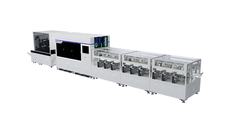
The equipment is composed of loading equipment, inspection equipment, and unloading equipment. The loading equipment is designed to remove broken fragments, which can remove the broken materials in advance. The testing equipment can efficiently and accurately identify the characteristics of silicon wafers and classify them according to customer requirements. The overall Modula design of unloading equipment can rapidly increase string types according to customer requirements.

 Equipment advantage
The industry's first 20000+ double half-piece detection
-The industry is the first two-half piece detection and sorting machine specially customized for HJT cell top customers. Two-half piece detection and sorting at the same time can reduce cost, increase efficiency, and help the development of the HJT process.
Large screen for dynamic data
- It can calculate the big data location of a defect by tool number and time and visually display the defect location through thermal profile to assist customers in process/abnormal analysis.
Double unloading location design
- Different from the traditional single unloading location design,the exclusive patent double unloading location design uses a single material box when the upper and lower switching easily, easily switching will not have DC
Data dynamics
- According to household demand display productivity yield.
- Real-time display of all boxes of materials.
- Real-time display of the current cutter materia distribution and sorting progress.
- Displays CPK for metered test items.
 Equipment characteristics
Fast sorting speed and high inspecting precision
- Capacity:≥14000pcs/h
- Fast sorting detection speed
- High accuracy
- Full scale inspection items≤30umEfficient and stable image acquisition with a self-developed software platform
- With the self-developed software platform, the German DALSA high-speed industrial linear array camera and acquisition card can acquire silicon line wafer images efficiently and stably, speeding up without losing frames.
Accurate detection based on 10 years of deep learning algorithm iteration in 3C industry
- More than 10 years of deep learning algorithm platform iteration in the 3c industry has accurately detected silicon wafer defects, and through the combination of traditional and deep learning, customers can easily and quickly configure the degraded chip discrimination criteria.
Special research on industry difficulties
- Special development of zero pressure frame of feeding table.
- Detection and recognition system of feeding casstte fragments.
- A special visual system for graded colour difference detection.
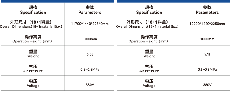
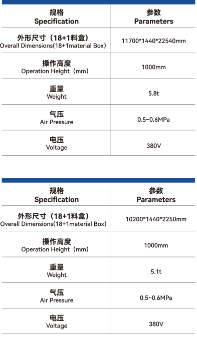
 Equipment specification


 Equipment parameter


 Test item
Thickness
Bow
Perforation
Stain
Edge Distance
Chamfer
Detritus removal
Fragment Removal
Electrical Resistivity
Micro Crack
Ttv
Saw Mark
Half-hole
Chipping
Diameter
Corner Chip
PN Type
Color Difference
Minority Carrier Lifetime(Optional)


